中文  |  English  |   The College of Information Science & Electronic Engineering  |  Zhejiang University  
HOME  Employment Contact us
Current position:Home > Research areas
High-speed large-scale silicon-based optical switching array
pubDate:2017-06-14 Click Browse:

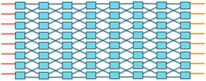
High-speed and large-capacity optical switching is of great significance in high-performance computers and modern optical communications. The research group designed and fabricated large-scale silicon-based high-speed optical switching devices using integrated silicon-based photonics technology. By improving the performance of individual devices and optimizing the system performance of the entire array, we have implemented nanosecond-level optical switching devices on the CMOS process line.

High-speed data exchange is very important in high-performance computers and modern optical communications, and the existing optical-to-optical switching method limits the transmission rate and increases the cost of data transmission, so direct optical-optical switching is of great significance. Silicon-based photonic devices are compatible with integrated circuit CMOS processes and can produce large-scale photonic integrated devices at low cost, making them the best choice for large-scale optical switching arrays.

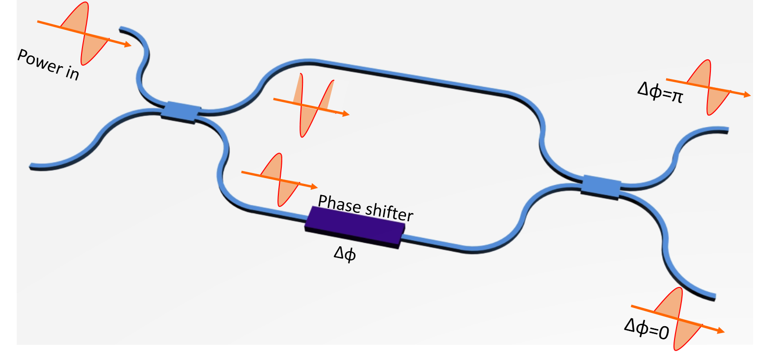
The Mach-Zehnder Interferometer (MZI) optical switch is the basic unit that constitutes the optical switching array. The working principle is to use the phase difference caused by the change of the refractive index of the two interfering arm waveguides. The phase difference can be controlled to achieve interference cancellation at the junction. The phase rises to achieve the switching function. According to the cause of the change in refractive index, it can be divided into a thermo-optic switch using a thermo-optic effect and an electro-optical switch using a plasma dispersion effect. The switching time of the thermo-optic switch is generally on the order of ms, and the switching time of the electro-optical switch is on the order of ns.


MZI switch structure diagram

The optical switch units are arranged in a certain topology to form a switch array with a certain function. According to the optical switch network blocking characteristics, it can be divided into two types of network structures: blocking type and non-blocking type. A blocked optical switch means that a new path is created to conflict with an established path, and the collision cannot be eliminated by reordering. The non-blocking optical switch means that the newly established path does not conflict with the existing path or when Blocking can be eliminated by arranging combinations when a conflict occurs.

The largest silicon-based optical switches currently reported internationally include a non-blocking 8x8 thermo-optic switch and a blocking type 8x8 electro-optical switch.

At present, our research includes the use of optical and electrical simulation software to simulate the structural parameters of the device, the design of the system structure, and the fabrication of devices in the CMOS process. We have implemented a 4x4 electro-optical switch with a switching time of nanoseconds and plan to implement a 16x16 electro-optic switch array by the end of 2015.


Blocking 8x8 network                                       Non-blocking 8x8 network


【Print this page】【Close this page】
Copyright © ZJU College of Information Science & Electronic Engineering Electro-Photonic Integrated Circuits Research Droup. All rights reserved.
ADD:618, Administration Building, 38 Zheda Road, Hangzhou, Zhejiang Province, 310027, P.R. China    POSTAL:310027  
TEL: 0571-87951673 E-mail:wuweike@zju.edu.cn